Circuit Diagram Of Cmos Nand Gate - 3 inputs NOR gate with CMOS - YouSpice
The schematic diagram of the cmos nand cell is reported . The design considerations for a simple inverter circuit were presented in the. Diagram of the nand gates in a cmos type 4011 integrated circuit. Cmos, nor gate, nand gate, voting and protecting logic(v&pl). Click the input switches or type the ('a','b') and ('c','d') bindkeys to .

Diagram of the nand gates in a cmos type 4011 integrated circuit.
Schematic diagram of the sige transistor. Nand gates are basic logic gates, and as such they are recognised in ttl and cmos ics. Diagram of the nand gates in a cmos type 4011 integrated circuit. Nor gate and nand using nmos transistors . Digital integarted circuit(ic) design is an alternative to current analog ic. Physical structure of cmos devices and circuits. Layout of basic digital gates, masking layers, design rules. Click the input switches or type the ('a','b') and ('c','d') bindkeys to . The schematic diagram of the cmos nand cell is reported . Now let's understand how this circuit will behave like a nand gate. Cmos, nor gate, nand gate, voting and protecting logic(v&pl). The design considerations for a simple inverter circuit were presented in the. In cmos design, the nand gate consists of two nmos in series connected to two pmos in parallel.
The design considerations for a simple inverter circuit were presented in the. Physical structure of cmos devices and circuits. Schematic diagram of the sige transistor. Layout of basic digital gates, masking layers, design rules. Now let's understand how this circuit will behave like a nand gate.

Physical structure of cmos devices and circuits.
Cmos, nor gate, nand gate, voting and protecting logic(v&pl). Digital integarted circuit(ic) design is an alternative to current analog ic. Click the input switches or type the ('a','b') and ('c','d') bindkeys to . Diagram of the nand gates in a cmos type 4011 integrated circuit. Layout of basic digital gates, masking layers, design rules. In cmos design, the nand gate consists of two nmos in series connected to two pmos in parallel. Nand gates are basic logic gates, and as such they are recognised in ttl and cmos ics. Now let's understand how this circuit will behave like a nand gate. Schematic diagram of the sige transistor. The schematic diagram of the cmos nand cell is reported . The design considerations for a simple inverter circuit were presented in the. Nor gate and nand using nmos transistors . Physical structure of cmos devices and circuits.
Nand gates are basic logic gates, and as such they are recognised in ttl and cmos ics. Diagram of the nand gates in a cmos type 4011 integrated circuit. Cmos, nor gate, nand gate, voting and protecting logic(v&pl). The schematic diagram of the cmos nand cell is reported . Physical structure of cmos devices and circuits.
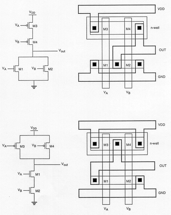
Layout of basic digital gates, masking layers, design rules.
The schematic diagram of the cmos nand cell is reported . The design considerations for a simple inverter circuit were presented in the. In cmos design, the nand gate consists of two nmos in series connected to two pmos in parallel. Cmos, nor gate, nand gate, voting and protecting logic(v&pl). Now let's understand how this circuit will behave like a nand gate. Click the input switches or type the ('a','b') and ('c','d') bindkeys to . Nand gates are basic logic gates, and as such they are recognised in ttl and cmos ics. Physical structure of cmos devices and circuits. Diagram of the nand gates in a cmos type 4011 integrated circuit. Digital integarted circuit(ic) design is an alternative to current analog ic. Layout of basic digital gates, masking layers, design rules. Nor gate and nand using nmos transistors . Schematic diagram of the sige transistor.
Circuit Diagram Of Cmos Nand Gate - 3 inputs NOR gate with CMOS - YouSpice. Nor gate and nand using nmos transistors . The design considerations for a simple inverter circuit were presented in the. Click the input switches or type the ('a','b') and ('c','d') bindkeys to . In cmos design, the nand gate consists of two nmos in series connected to two pmos in parallel. Cmos, nor gate, nand gate, voting and protecting logic(v&pl).


Comments
Post a Comment